In the world of embedded processors, power consumption is critical; hence, most sophisticated embedded processors provide mechanisms to power down any resources that are not required for a particular application.
http://blog.mark-stevens.co.uk/category/stm32/
Clocks
Three different clock sources can be used to drive the system clock (SYSCLK):
• HSI oscillator clock – High Speed Internal
• HSE oscillator clock – High Speed External
• Main PLL (PLL) clock
The devices have the two following secondary clock sources:
• 32 kHz low-speed internal RC (LSI RC)
which drives the independent watchdog and, optionally, the RTC used for Auto-wakeup from the Stop/Standby mode.
• 32.768 kHz low-speed external crystal (LSE crystal) which optionally drives the RTC clock (RTCCLK)
The first three clocks are used to drive the system clock for the microcontroller. The final two are low speed clocks and are primarily used to drive the watchdogs.
Each clock source can be switched on or off independently when it is not used, to optimize power consumption.
HSI
After reset, the STM32 enables the HSI oscillator. This has a relatively low accuracy, only 1%, but is suitable for most applications. Using the HSI oscillator eliminates the need for an external clock in the final circuit design. On the STM32F4, the HSI oscillator has a clock speed of 16 MHz.
HSE
The STM32 can operate using an external clock circuit. It is possible to design an external clock to run with a greater accuracy than the internal HSI clock enabling finer control of the operating parameters of the final circuit. The exact specification of the external clock frequency varies but is typically 4-16 MHz. The STM32F4 Discovery Board has a built in external oscillator circuit fitted with a 8 MHz crystal.
PLL
The PLL is used to multiply it’s input clock source by a factor varying between 2 to 16. The input of the PLL is one of HSI, HSE or HSE/2. It is important to note that the configuration of the PLL cannot be changed once it has been enabled.
LSI
The LSI is a low power clock used for the watchdog timers.
LSE
The LSE is powered by an external 32.768 KHz clock. This provides a method of providing a low speed accurate clock for the real time clock.
Peripheral clocks
Over the last half-decade, dramatically lowering current draw has been a goal for most microcontroller manufacturers. One of the techniques used to achieve this is to switch off on-chip peripherals by removing access to their master clocks. On the STM32 devices, these clocks are known as the hardware and peripheral clocks and are controlled by the RCC (Reset and Clock Control) group of registers. Since there are more than 32 on chip peripherals, there are actually two registers used to switch on a clock: RCC_AHB1ENR and RCC_AHB2ENR for the Hardware clock, APB for the Peripheral clock. The clock is controlled by set/reset registers, so to turn a system on you set a bit in the ENR register, and to turn that same peripheral off you set the bit in the corresponding RCC_AHBxRSTR register.
Clock Distribution
Once the clock source has been selected it is necessary to configure the internal system and peripheral clocks. The internal clocks are:
- System Clock
- Advanced High Performance Bus (AHB)
- Low speed Advanced Peripheral Bus (APB1)
- High speed Advanced Peripheral Bus (APB2)
Each of these clocks can be scaled using prescalers.
System Clock
The system clock is used to determine the speed at which instructions are executed and has a maximum speed of 168MHz.
Advanced High Performance Bus (AHB)
Derived from the system clock, this bus has a maximum speed of 168MHz.
Low speed Advanced Peripheral Bus (APB1)
Derived from AHB, this bus has a maximum speed of 42MHz.
High speed Advanced Peripheral Bus (APB2)
Derived from AHB, this clock has a maximum frequency of 84MHz.
Non-System Clock Peripherals
A number of the peripheral clocks are not derived from the system clock but have their own independent source.
The STM32 has a complex clock distribution network which ensures that only those peripherals that are actually needed are powered. This system, called Reset and Clock Control (RCC) is supported by the firmware module stm32f4xx_rcc.[ch].
While this module can be used to control the main system clocks and PLLs, any required configuration of those is handled by the startup code. Our concern here is simply with enabling the peripheral clocks.
extracting from stm32f4xx_rcc.c :
RCC_AHB1Periph_GPIOA: GPIOA clock
RCC_AHB1Periph_GPIOB: GPIOB clock
RCC_AHB1Periph_GPIOC: GPIOC clock
RCC_AHB1Periph_GPIOD: GPIOD clock
RCC_AHB1Periph_GPIOE: GPIOE clock
RCC_AHB1Periph_GPIOF: GPIOF clock
RCC_AHB1Periph_GPIOG: GPIOG clock
RCC_AHB1Periph_GPIOG: GPIOG clock
RCC_AHB1Periph_GPIOI: GPIOI clock
RCC_AHB1Periph_CRC: CRC clock
RCC_AHB1Periph_BKPSRAM: BKPSRAM interface clock
RCC_AHB1Periph_CCMDATARAMEN CCM data RAM interface clock
RCC_AHB1Periph_DMA1: DMA1 clock
RCC_AHB1Periph_DMA2: DMA2 clock
RCC_AHB1Periph_ETH_MAC: Ethernet MAC clock
RCC_AHB1Periph_ETH_MAC_Tx: Ethernet Transmission clock
RCC_AHB1Periph_ETH_MAC_Rx: Ethernet Reception clock
RCC_AHB1Periph_ETH_MAC_PTP: Ethernet PTP clock
RCC_AHB1Periph_OTG_HS: USB OTG HS clock
RCC_AHB1Periph_OTG_HS_ULPI: USB OTG HS ULPI clock
.
RCC_AHB2Periph_DCMI : DCMI clock
RCC_AHB2Periph_CRYP : CRYP clock
RCC_AHB2Periph_HASH : HASH clock
RCC_AHB2Periph_RNG : RNG clock
RCC_AHB2Periph_OTG_FS : USB OTG FS clock
.
RCC_APB1Periph_TIM2 : TIM2 clock
RCC_APB1Periph_TIM3 : TIM3 clock
RCC_APB1Periph_TIM4 : TIM4 clock
RCC_APB1Periph_TIM5 : TIM5 clock
RCC_APB1Periph_TIM6 : TIM6 clock
RCC_APB1Periph_TIM7 : TIM7 clock
RCC_APB1Periph_TIM12 : TIM12 clock
RCC_APB1Periph_TIM13 : TIM13 clock
RCC_APB1Periph_TIM14 : TIM14 clock
RCC_APB1Periph_WWDG : WWDG clock
RCC_APB1Periph_SPI2 : SPI2 clock
RCC_APB1Periph_SPI3 : SPI3 clock
RCC_APB1Periph_USART2 : USART2 clock
RCC_APB1Periph_USART3 : USART3 clock
RCC_APB1Periph_UART4 : UART4 clock
RCC_APB1Periph_UART5 : UART5 clock
RCC_APB1Periph_I2C1 : I2C1 clock
RCC_APB1Periph_I2C2 : I2C2 clock
RCC_APB1Periph_I2C3 : I2C3 clock
RCC_APB1Periph_CAN1 : CAN1 clock
RCC_APB1Periph_CAN2 : CAN2 clock
RCC_APB1Periph_PWR : PWR clock
RCC_APB1Periph_DAC : DAC clock
.
RCC_APB2Periph_TIM1: TIM1 clock
RCC_APB2Periph_TIM8: TIM8 clock
RCC_APB2Periph_USART1: USART1 clock
RCC_APB2Periph_USART6: USART6 clock
RCC_APB2Periph_ADC1: ADC1 clock
RCC_APB2Periph_ADC2: ADC2 clock
RCC_APB2Periph_ADC3: ADC3 clock
RCC_APB2Periph_SDIO: SDIO clock
RCC_APB2Periph_SPI1: SPI1 clock
RCC_APB2Periph_SYSCFG: SYSCFG clock
RCC_APB2Periph_TIM9: TIM9 clock
RCC_APB2Periph_TIM10: TIM10 clock
RCC_APB2Periph_TIM11: TIM11 clock
.
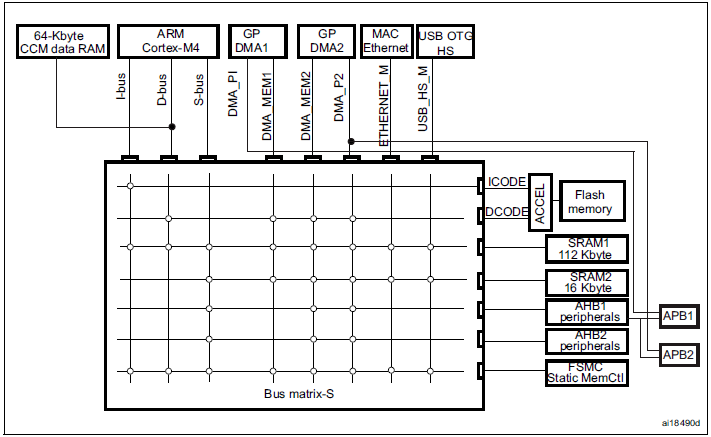
System architecture
Bus Matrix
The bus matrix interconnects 8 bus masters with 7 slaves:

In STM32F405xx/07xx and STM32F415xx/17xx, the main system consists of 32-bit multilayer AHB bus matrix that interconnects:
The main system consists of 32-bit multilayer AHB bus matrix that interconnects:
• Eight masters:
– Cortex™-M4 with FPU core I-bus, D-bus and S-bus
– DMA1 memory bus
– DMA2 memory bus
– DMA2 peripheral bus
– Ethernet DMA bus
– USB OTG HS DMA bus
• Seven slaves:
– Internal Flash memory ICode bus
– Internal Flash memory DCode bus
– Main internal SRAM1 (112 KB)
– Auxiliary internal SRAM2 (16 KB)
– AHB1 peripherals including AHB to APB bridges and APB peripherals
– AHB2 peripherals
– FSMC
The bus matrix provides access from a master to a slave, enabling concurrent access and efficient operation even when several high-speed peripherals work simultaneously. The 64-Kbyte CCM (core coupled memory) data RAM is not part of the bus matrix and can be accessed only through the CPU. This architecture is shown in Figure :
System architecture for STM32F405xx/07xx and STM32F415xx/17xx devices
.
.
.
.
.
.
.
.
.
.
.
.
.
.
.
.
.
